Netherlands-Japan Semiconductor Talent Program
Osaka-Tokyo-Hokaido
14-18 December 2026
Why join? // Content of lectures // Lecturers // Venues
About the school
The Netherlands-Japan Semiconductor Talent Program is an immersive, interdisciplinary program for Japanese master’s degree and accelerated master's degree students interested in learning more about the semiconductor industry and exploring potential career pathways within this dynamic field.
The program will take place December 14–18, 2026. Selected participants are expected to commit to the full program in Osaka (14 December), 15-16 December (Tokyo) or 18 December (Hokkaido) and attend all scheduled programming of the day. Participating students will receive a Certificate of Participation.

Semiconductors power the technologies shaping our future
Semiconductors are foundational to technologies revolutionizing society, ranging from AI, advanced computing, smart mobility, renewable energy systems, advanced healthcare, electronics, and more.
A complex ecosystem of universities, suppliers, customers, research institutes and governments are working together to drive innovation across the semiconductor value chain – from manufacturing equipment, chip design, fabrication and assembly, accelerated through advancements in materials, software, heterogenous integration and AI.

Organization: ISTP, a broader semicon talent initiative
The Netherlands-Japan Semiconductor Talent Program is one of four education programs delivered in 2026 under the International Semiconductor Talent Program (ISTP), the Netherlands' broader effort to connect students with the global semiconductor ecosystem. ISTP members are the Ministry of Foreign Affairs, the Technical University of Eindhoven, ASML, NXP and ASM. Building on this momentum, plans are underway to deepen and expand the Netherlands-Japan Semiconductor Talent Program in 2027.
Why Join?
Participants will gain a broader understanding of the global significance of the semiconductor ecosystem, hear directly from academic and industry experts, and see how different disciplines and career paths contribute to semiconductor technology and innovation. The program will include opportunities to engage with leading industry partners, with two full days hosted by Osaka University, Tokyo University and Hokkaido University, respectively.
Participants do not need to have specialized semiconductor experience. We are seeking students from a range of STEM backgrounds who are curious about the industry, interested in understanding how their knowledge and skills may apply to the semiconductor ecosystem, and motivated to explore future career opportunities in the field.
By participating, students will gain industry exposure, professional connections, a deeper understanding of the semiconductor value chain, and insight into potential career and professional development opportunities within the semiconductor industry.
Deep dive into challenges and opportunities across the semiconductor value chain by hearing from expert lectures
See first-hand company operations with facility visits & study tours
Learn about opportunities for students and graduates during career-focused sessions
Network with semiconductor professionals
““Two countries. One ambition.
A new generation of semiconductor talent.””
Content of lectures
Domain 1
Process Technology/material/plasma
Building on the atomic-scale processing techniques, the lecture explores how they enable emerging materials and device concepts for next-generation semiconductor technologies.
Three representative material systems are discussed: two-dimensional semiconductors for future transistors, conductive oxide semiconductors for advanced memory architectures, and ferroelectric hafnium zirconium oxide for novel memory devices. Starting from their applications, we examine how material properties and device requirements translate into challenges in deposition, composition control, interfaces, and conformality. These examples illustrate the connection between atomic-scale processing, materials engineering, semiconductor manufacturing equipment, and device performance.
Domain 2
Equipment/components/
electronics/mechatronics
This exclusive 4-hour lecture offers a comprehensive insight into this unique innovation engine.
We will explore the historical background, fundamental design principles, industrial relevance, and the latest technological advancements shaping the future of mechatronics. The lecture is structured into three core components:
1. Foundation & History
An examination of how pioneers within Philips laid the groundwork for the mechatronic revolution through exact constraint design. We will discuss how this philosophy was advanced by researchers like Maarten Steinbuch (first at Philips Research and later as a professor at TU/e) into today’s standards for high-precision engineering.
2. Relevance & Ecosystem
The evolution of Philips spin-offs into the current Brainport ecosystem of open innovation. We will highlight the powerful symbiosis between Eindhoven University of Technology (TU/e), applied research institutes, and the industry, illustrating why this mechatronic approach is vital to the global semiconductor and healthcare sectors, with special focus on the role of ASML.
3. Future Developments
An overview of next-generation technologies, ranging from active vibration isolation and thermomechanical control at the picometer level, to the integration of Artificial Intelligence (AI) in complex, autonomous mechatronic systems.
Lecturers
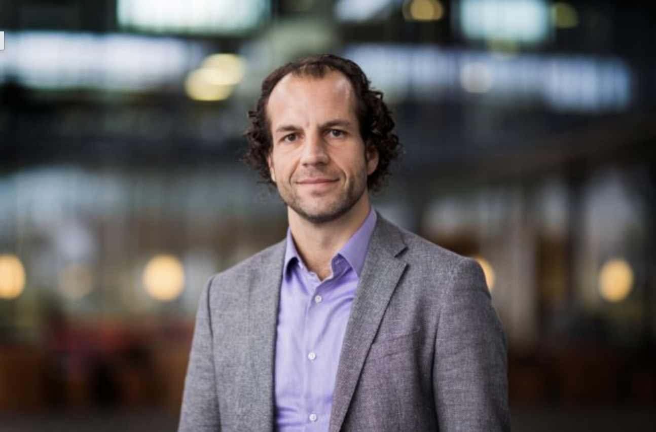
Erwin Kessels
Full Professor, Department of Applied Physics, Eindhoven University of Technology
Erwin Kessels is a full professor at the Department of Applied Physics of Eindhoven University of Technology (TU/e). He is also the scientific director of the NanoLab@TU/e facilities which provides full-service and open-access clean room infrastructure for R&D in nanotechnology. Erwin’s research interests cover the field of synthesis of ultrathin films and nanostructures using methods such as (plasma-enhanced) chemical vapor deposition (CVD) and atomic layer deposition (ALD) for a wide variety of applications, mostly within the areas of nanoelectronics and photovoltaics. Within the field of ALD, he has contributed most prominently by his work on plasma-assisted ALD, his research related to ALD for photovoltaics, and ALD for nanopatterning (including area-selective ALD). Currently, Erwin is focusing his research mostly on atomic scale processing, a field which is believed to grow in importance quickly in the next decade, for a wide variety of application domains.
w.m.m.kessels@tue.nl | https://www.tue.nl/en/research/researchers/erwin-kessels
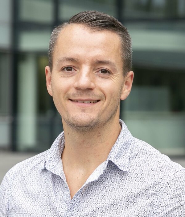
Bart Macco
Assistant Professor, Department of Applied Physics, Eindhoven University of Technology
Bart Macco is an Assistant Professor in the Plasma & Materials Processing (PMP) group at Eindhoven University of Technology (TU/e). His research focuses on atomic layer deposition (ALD), atomic-scale processing and semiconductor interface physics. His work includes conductive oxide semiconductors, ferroelectric HfZrO thin films, high-k dielectrics and passivation layers for graphene and III–V semiconductors, and atomically thin transition-metal dichalcogenides.
b.macco@tue.nl https://www.tue.nl/en/research/researchers/bart-macco
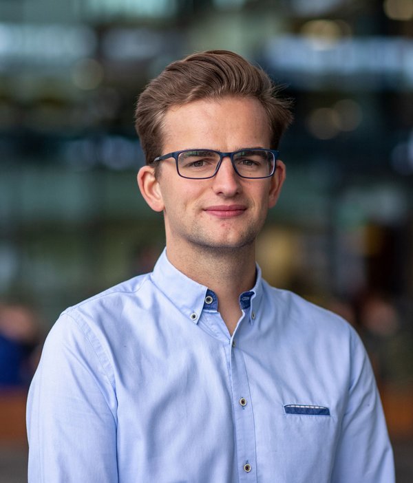
Ron de Bruijn
Assistant Professor, Department of Mechanical Engineering, Eindhoven University of Technology
Ron de Bruijn obtained both his BSc (Magna Cum Laude) and MSc (Summa Cum Laude) in Electromechanical Engineering Technology from KU Leuven (Geel campus), Belgium. During his MSc graduation project, “Cost Effective Design of the Pellicle Hardware”, conducted in collaboration with ASML, he developed a novel and more cost-effective hardware concept for pellicle integration in lithography systems. This work resulted in a patent publication and was awarded the Best MSc Thesis in Electromechanical Engineering Technology. He received his PhD degree in Mechanical Engineering from Eindhoven University of Technology (TU/e) in 2025. His PhD research focused on the design and mechatronic architecture of a piezoelectric wafer stage for electron beam inspection systems, developed in close collaboration with ASML. The work combined precision mechanical design, piezoelectric actuation, system thinking, control, and resulted in 3 patent publications.
r.g.c.d.bruijn@tue.nl https://www.tue.nl/en/research/researchers/ron-de-bruijn
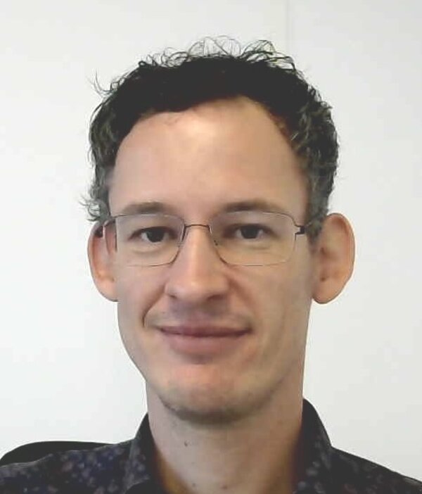
Kees Verbaan
Hybrid Teacher, Department of Mechanical Engineering, Eindhoven University of Technology
“With industrial experience in the field of mechatronics design, I dedicated myself to performing research in this field, with a focus on system accuracy and mechanical design in combination with dynamics and motion control. Mainly via student assignments I'm attempting to execute research with our industrial partners.”
c.a.m.verbaan@tue.nl https://www.tue.nl/en/research/researchers/kees-verbaan
Venues
Osaka University
14 December
Icho Hall
PM
Tokyo University
15-16 December
Haseko-Kuma Hall
(Engineering Building 11,
Faculty of Engineering,
The University of Tokyo
Address: 7-3-1 Hongo, Bukyo-ku, Tokyo
Map: Building no. 84 on the map
https://www.u-tokyo.ac.jp/content/400020145.pdf
Hokkaido University
18 December
PM